- 您现在的位置:买卖IC网 > Sheet目录329 > IDT70V3579S5DRI (IDT, Integrated Device Technology Inc)IC SRAM 1.125MBIT 5NS 208QFP
IDT70V3579S
High-Speed 32K x 36 Dual-Port Synchronous Pipelined Static RAM
Industrial and Commercial Temperature Ranges
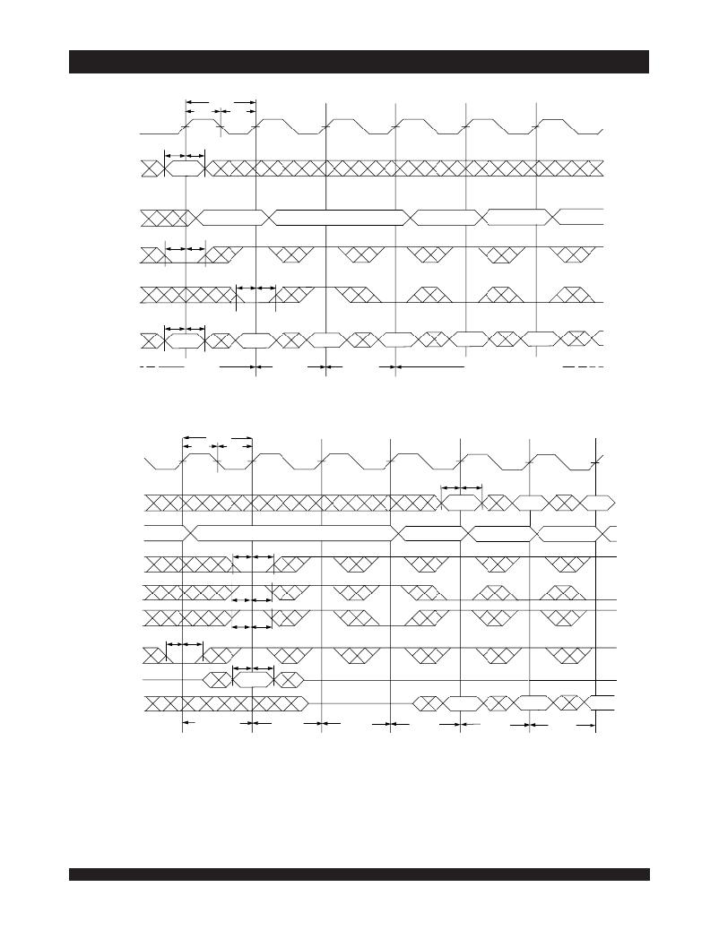
Timing Waveform of Write with Address Counter Advance (1)
t CYC2
CLK
t CH2
t CL2
t SA
t HA
ADDRESS
An
INTERNAL (3)
ADDRESS
An (7)
An + 1
An + 2
An + 3
An + 4
t SAD t HAD
ADS
t SCN t HCN
CNTEN
t SD t HD
DATA IN
Dn
Dn + 1
Dn + 1
Dn + 2
Dn + 3
Dn + 4
WRITE
EXTERNAL
ADDRESS
WRITE WRITE
WITH COUNTER COUNTER HOLD
WRITE WITH COUNTER
4830 drw 12
Timing Waveform of Counter Reset (2)
t CYC2
t CH2
t CL2
CLK
t SA t HA
(4)
ADDRESS
An
An + 1
An + 2
INTERNAL (3)
ADDRESS
Ax
0
1
An
An + 1
t SW t HW
R/ W
ADS
CNTEN
t SRST t HRST
t SAD t HAD
t SCN t HCN
CNTRST
DATA IN
(5)
t SD
t HD
D 0
DATA OUT
Q 0
Q 1
Qn
COUNTER
RESET
(6)
WRITE
ADDRESS 0
READ
ADDRESS 0
READ
ADDRESS 1
READ
ADDRESS n
READ
ADDRESS n+1
NOTES:
1. CE 0 , BE n , and R/ W = V IL ; CE 1 and CNTRST = V IH .
4830 drw 13
2. CE 0 , BE n = V IL ; CE 1 = V IH .
3. The "Internal Address" is equal to the "External Address" when ADS = V IL and equals the counter output when ADS = V IH .
4. Addresses do not have to be accessed sequentially since ADS = V IL constantly loads the address on the rising edge of the CLK; numbers are for reference
use only.
5. Output state (High, Low, or High-impedance) is determined by the previous cycle control signals.
6. No dead cycle exists during counter reset. A READ or WRITE cycle may be coincidental with the counter reset cycle: A DDR 0 will be accessed. Extra cycles
are shown here simply for clarification.
7. CNTEN = V IL advances Internal Address from ‘An’ to ‘An +1’. The transition shown indicates the time required for the counter to advance. The ‘An +1’Address is
written to during this cycle.
14
6.42
发布紧急采购,3分钟左右您将得到回复。
相关PDF资料
IDT70V3599S133DRI
IC SRAM 4MBIT 133MHZ 208QFP
IDT70V37L20PFI
IC SRAM 576KBIT 20NS 100TQFP
IDT70V38L15PFG
IC SRAM 1.125MBIT 15NS 100TQFP
IDT70V525ML55BZI
IC SRAM 128KBIT 55NS 144FBGA
IDT70V5388S166BGI
IC SRAM 1.125MBIT 166MHZ 272BGA
IDT70V631S10PRFG
IC SRAM 4MBIT 10NS 128TQFP
IDT70V639S12PRFI
IC SRAM 2.25MBIT 12NS 128TQFP
IDT70V659S12DRI
IC SRAM 4MBIT 12NS 208QFP
相关代理商/技术参数
IDT70V3579S6BC
功能描述:IC SRAM 1.125MBIT 6NS 256BGA RoHS:否 类别:集成电路 (IC) >> 存储器 系列:- 标准包装:3,000 系列:- 格式 - 存储器:EEPROMs - 串行 存储器类型:EEPROM 存储容量:8K (1K x 8) 速度:400kHz 接口:I²C,2 线串口 电源电压:1.7 V ~ 5.5 V 工作温度:-40°C ~ 85°C 封装/外壳:8-SOIC(0.154",3.90mm 宽) 供应商设备封装:8-SOIC 包装:带卷 (TR)
IDT70V3579S6BC8
功能描述:IC SRAM 1.125MBIT 6NS 256BGA RoHS:否 类别:集成电路 (IC) >> 存储器 系列:- 标准包装:1,000 系列:- 格式 - 存储器:RAM 存储器类型:SRAM - 双端口,同步 存储容量:1.125M(32K x 36) 速度:5ns 接口:并联 电源电压:3.15 V ~ 3.45 V 工作温度:-40°C ~ 85°C 封装/外壳:256-LBGA 供应商设备封装:256-CABGA(17x17) 包装:带卷 (TR) 其它名称:70V3579S5BCI8
IDT70V3579S6BCI
制造商:Integrated Device Technology Inc 功能描述:IC SRAM 1.125MBIT 6NS 256CABGA
IDT70V3579S6BCI8
制造商:Integrated Device Technology Inc 功能描述:IC SRAM 1.125MBIT 6NS 256CABGA
IDT70V3579S6BF
功能描述:IC SRAM 1.125MBIT 6NS 208FBGA RoHS:否 类别:集成电路 (IC) >> 存储器 系列:- 标准包装:3,000 系列:- 格式 - 存储器:EEPROMs - 串行 存储器类型:EEPROM 存储容量:8K (1K x 8) 速度:400kHz 接口:I²C,2 线串口 电源电压:1.7 V ~ 5.5 V 工作温度:-40°C ~ 85°C 封装/外壳:8-SOIC(0.154",3.90mm 宽) 供应商设备封装:8-SOIC 包装:带卷 (TR)
IDT70V3579S6BF8
功能描述:IC SRAM 1.125MBIT 6NS 208FBGA RoHS:否 类别:集成电路 (IC) >> 存储器 系列:- 标准包装:1,000 系列:- 格式 - 存储器:RAM 存储器类型:SRAM - 双端口,同步 存储容量:1.125M(32K x 36) 速度:5ns 接口:并联 电源电压:3.15 V ~ 3.45 V 工作温度:-40°C ~ 85°C 封装/外壳:256-LBGA 供应商设备封装:256-CABGA(17x17) 包装:带卷 (TR) 其它名称:70V3579S5BCI8
IDT70V3579S6DR
功能描述:IC SRAM 1.125MBIT 6NS 208QFP RoHS:否 类别:集成电路 (IC) >> 存储器 系列:- 标准包装:3,000 系列:- 格式 - 存储器:EEPROMs - 串行 存储器类型:EEPROM 存储容量:8K (1K x 8) 速度:400kHz 接口:I²C,2 线串口 电源电压:1.7 V ~ 5.5 V 工作温度:-40°C ~ 85°C 封装/外壳:8-SOIC(0.154",3.90mm 宽) 供应商设备封装:8-SOIC 包装:带卷 (TR)
IDT70V3589S133BC
功能描述:IC SRAM 2MBIT 133MHZ 256BGA RoHS:否 类别:集成电路 (IC) >> 存储器 系列:- 标准包装:3,000 系列:- 格式 - 存储器:EEPROMs - 串行 存储器类型:EEPROM 存储容量:8K (1K x 8) 速度:400kHz 接口:I²C,2 线串口 电源电压:1.7 V ~ 5.5 V 工作温度:-40°C ~ 85°C 封装/外壳:8-SOIC(0.154",3.90mm 宽) 供应商设备封装:8-SOIC 包装:带卷 (TR)
